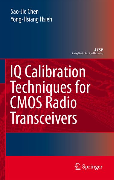
IQ Calibration Techniques for CMOS Radio Transceivers
-
- Hardcover
- Taschenbuch ausgewählt
-
Sprache:Englisch
92,99 €
inkl. gesetzl. MwSt.,
Beschreibung
Produktdetails
Einband
Taschenbuch
Erscheinungsdatum
30.11.2010
Abbildungen
XIX, 89 p.
Verlag
Springer NetherlandSeitenzahl
89
Maße (L/B/H)
23,5/15,5/0,7 cm
Gewicht
184 g
Auflage
1. Auflage
Sprache
Englisch
ISBN
978-90-481-7279-5
In the market of wireless communication, high data-rate transmission and high spectral efficiency have been the trend. The IEEE 802.11 a/g standards working at 5GHz/2.4GHz ISM bands can support data rate up to 54Mbits/s using OFDM modulation. The newly proposed 802.11n technology now uses 64-QAM to achieve higher spectral efficiency. The DVB and many other systems will also use QAM for its data transmission.
The cost of achieving this higher spectral efficiency using higher order QAM is that the transmitter and receiver requires a higher signal to noise ratio (SNR) with the same level of error rate performance (relative to a baseline BPSK, QPSK and other systems). One of the dominant vectors on SNR degradation is I/Q image rejection (I/Q gains and phases imbalance).
There are a lot of factors that degrade the matching of gains and phases between I/Q signals: the instinct layout mismatch, the random mismatch of the devices, the different temperatures over the I/Q signal paths. IQ Calibration Techniques For CMOS Radio Transceivers describes a fully-analog compensation technique without baseband circuitry to control the calibration process. This book will use an 802.11g transceiver design as an example to give a detailed description on the I/Q gains and phases imbalance auto-calibration mechanism.
Noch keine Bewertungen vorhanden
Verfassen Sie die erste Bewertung zu diesem Artikel
Helfen Sie anderen Kundinnen und Kunden durch Ihre Meinung.
Kurze Frage zu unserer Seite
Vielen Dank für Ihr Feedback
Wir nutzen Ihr Feedback, um unsere Produktseiten zu verbessern. Bitte haben Sie Verständnis, dass wir Ihnen keine Rückmeldung geben können. Falls Sie Kontakt mit uns aufnehmen möchten, können Sie sich aber gerne an unseren Kund*innenservice wenden.
zum Kundenservice