Band 54
Polycrystalline Semiconductors II Proceedings of the Second International Conference Schwäbisch Hall, Fed. Rep. of Germany, July 30–August 3,1990
Aus der Reihe
Springer Proceedings in Physics
-
- Englisch ausgewählt
97,99 €
inkl. gesetzl. MwSt.,
Beschreibung
Produktdetails
Einband
Taschenbuch
Erscheinungsdatum
06.12.2011
Herausgeber
Jürgen H. Werner + weitereVerlag
Springer BerlinSeitenzahl
549
Maße (L/B/H)
23,5/15,5/3,1 cm
Gewicht
850 g
Auflage
1991
Sprache
Englisch
ISBN
978-3-642-76387-8
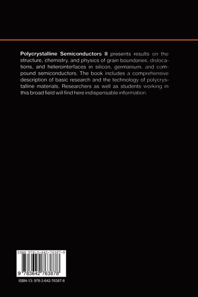
This book contains papers that were presented at the International Conference on Polycrystalline Semiconductors - Grain Boundaries, Dislocations and Het erointerfaces - (POLYSE '90), which was held in Schwabisch Hall, FRG, from July 30 to August 3, 1990. This conference was a satellite conference of the 20th International Conference on the Physics of Semiconductors. POLYSE '90, like its predecessor POLYSE '88, brought together scientists from research in stitutions and industrial laboratories with a view to bridging the gap between fundamental and technological aspects of polycrystalline semiconductors. With this aim, a total of 14 recognized scientists from universities and in dustry were invited to review their fields of interest. The expert presentations of these scientists were complemented by contributed papers and poster con tributions, the authors of which were additionally allowed four minutes for an oral summary. This combination of different types of presentation led to very lively and stimulating discussions.
Kundinnen und Kunden meinen
Verfassen Sie die erste Bewertung zu diesem Artikel
Helfen Sie anderen Kund*innen durch Ihre Meinung
Kurze Frage zu unserer Seite
Vielen Dank für Ihr Feedback
Wir nutzen Ihr Feedback, um unsere Produktseiten zu verbessern. Bitte haben Sie Verständnis, dass wir Ihnen keine Rückmeldung geben können. Falls Sie Kontakt mit uns aufnehmen möchten, können Sie sich aber gerne an unseren Kund*innenservice wenden.
zum Kundenservice